In the semiconductor industry, Exyte is famous for its cleanrooms and controlled environments. But sometimes clean is not enough. Sometimes clients require a room that can't even be penetrated by electromagnetic radiation. This is where the experts at Exyte Technology get to work. The result of their creativity and efforts help to shrink the technology nodes of semiconductors down to less than five nanometers. This will make electronic devices even more powerful and compact.
The white box standing in the production hall in Renningen, a town just outside Stuttgart, could be anything. An oversized refrigerator? The module of a space station? An ancient computer? Not exactly.
Thanks to this “electromagnetic interference shielding chamber” for scanning electron microscope applications (yes, that's a long name, let’s just call it a chamber from now on), an Exyte client can now produce perfect semiconductors that are even smaller, faster, and more efficient. Exyte developed the chamber together with the client, from vision to perfect solution.
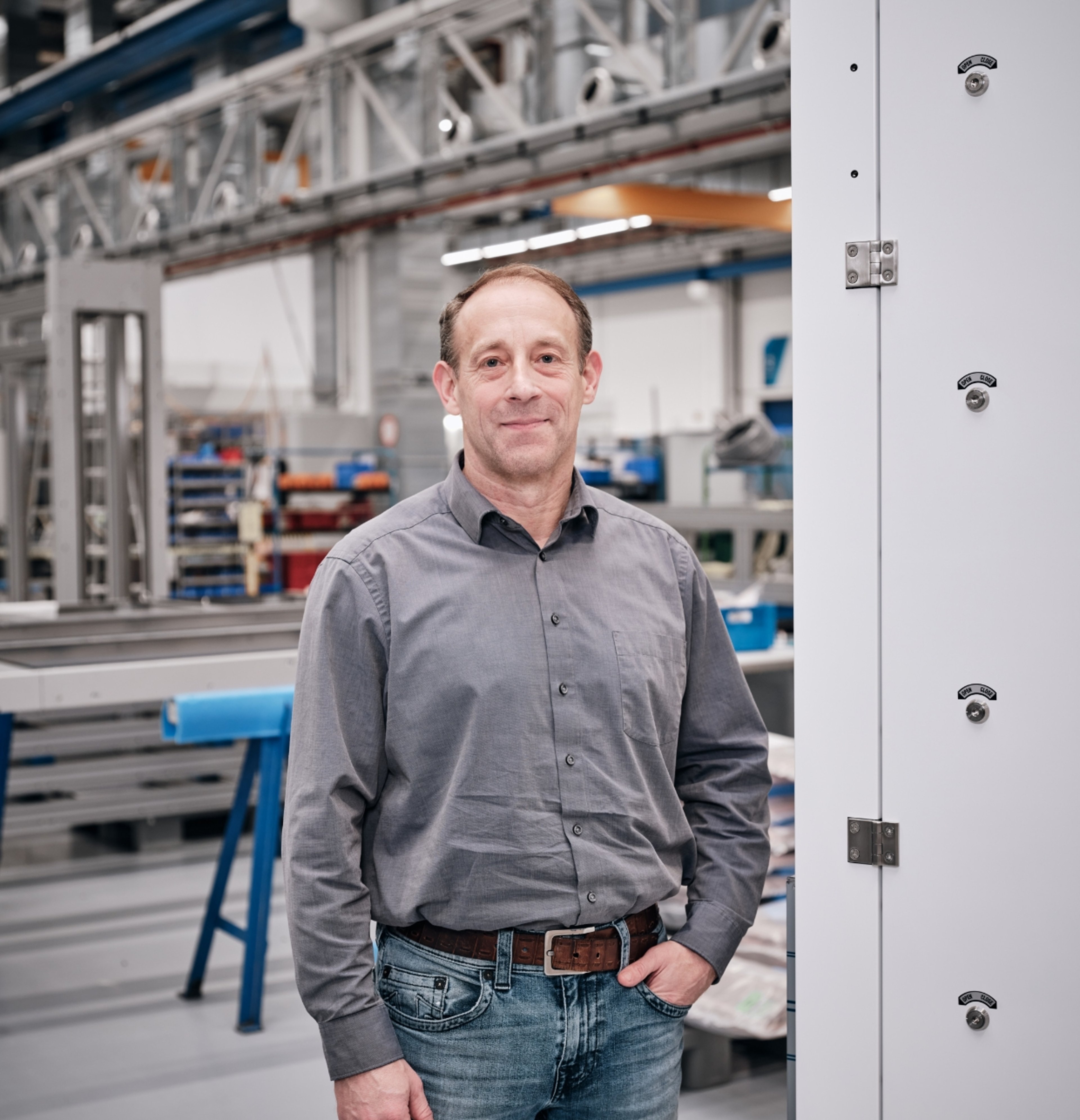
Semiconductors are manufactured in multiple layers that are coated, exposed, and etched several times. The foundation is a wafer: a round, flat disc made of silicon. Since semiconductors are extremely sensitive and have become so small that they are measured in nanometers (a nanometer is the millionth part of a millimeter, a human hair is between 50,000 and 100,000 nanometers thick), the wafer must be flawless. “Even a speck of dust can disrupt entire production processes,\" explains Fabian Ankele, Technical Product Manager for Exyte Technology.
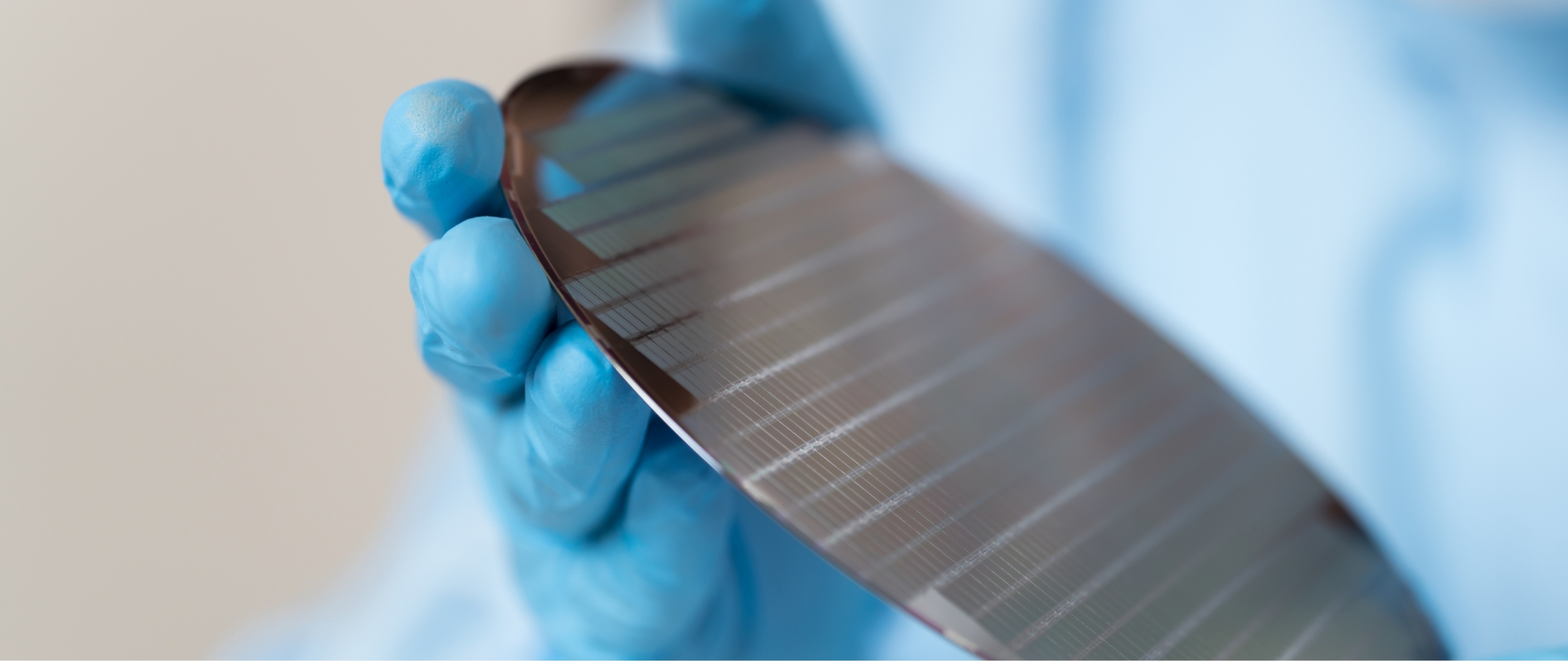
Semiconductors are manufactured in multiple layers that are coated, exposed, and etched several times. The foundation is a wafer: a round, flat disc made of silicon. Since semiconductors are extremely sensitive and have become so small that they are measured in nanometers (a nanometer is the millionth part of a millimeter, a human hair is between 50,000 and 100,000 nanometers thick), the wafer must be flawless. “Even a speck of dust can disrupt entire production processes," explains Fabian Ankele, Technical Product Manager for Exyte Technology.
The clean room within the clean room
“It's more or less the only chamber of its kind on the market so far."
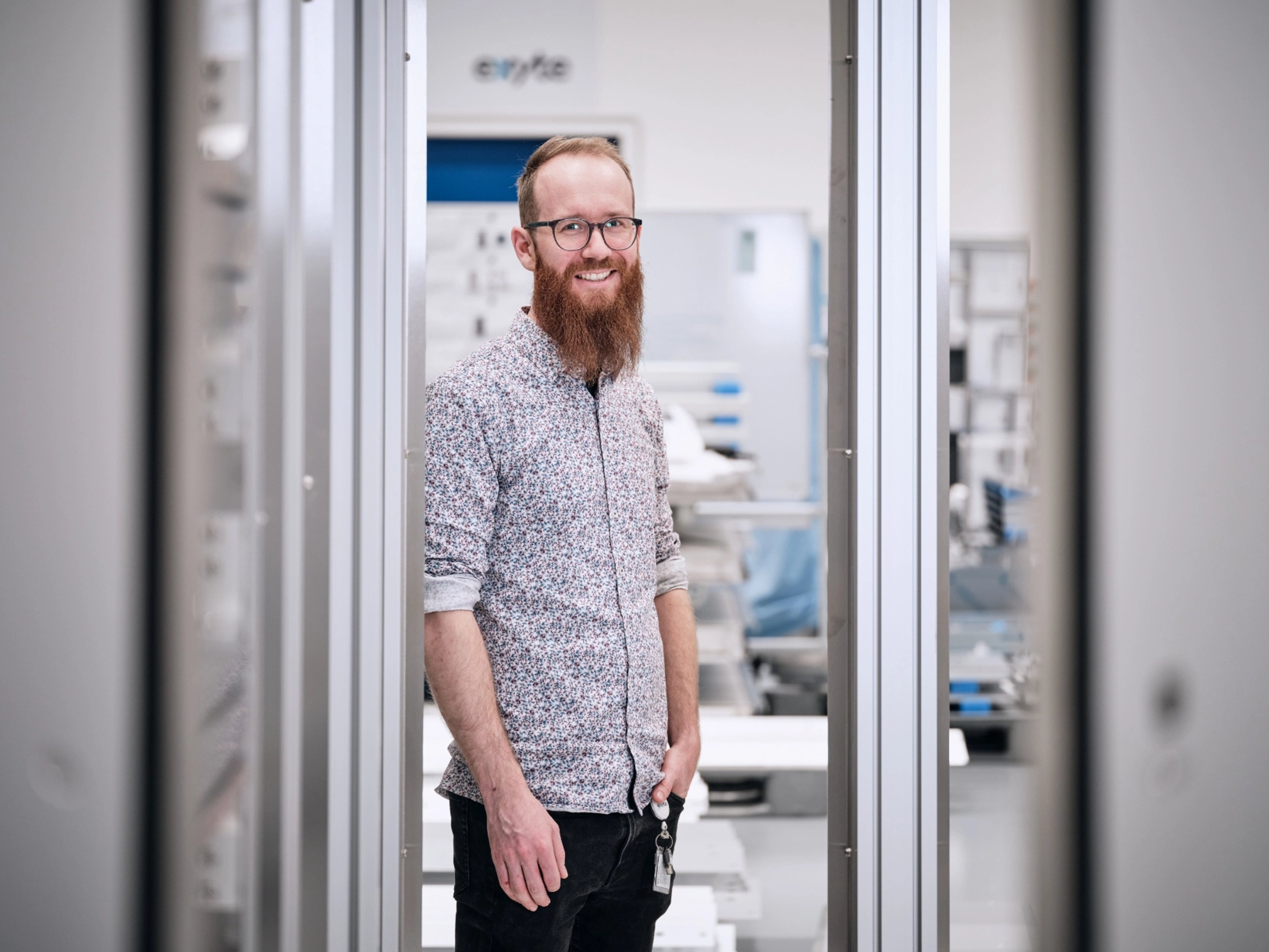
There is an additional vacuum chamber inside the shielding chamber. This is maintained even when the wafers are inserted by robots. "That was perhaps the biggest challenge. How do we maintain the vacuum and keep the electromagnetic radiation out when something enters the chamber?" asks Steffen Kühnle, Mechanical Designer at Exyte Technology. For this purpose, the engineers in Renningen developed special interfaces that are connected to the chamber. "It's more or less the only chamber of its kind on the market so far."
Capable of serial production
Another advantage of Exyte’s chamber over other scanning electron microscope systems is that it saves a lot of space. "Our chamber really only requires the space that the electron microscope needs. That saves the client space and therefore money,” says Ankele. Taking advantage of this leading edge, Exyte commenced serial production of the chamber.

Excited to build a better future with us?
ARE YOU LOOKING FOR:
.jpeg?w=3840)
Newsroom
.jpeg?w=3840)
Fostering of sustainability
100+ Years of history
ARE YOU LOOKING FOR:
.jpeg?w=3840)
World of Exyte
/221211_PHO_BLS_Pharma_1.jpeg?w=3840)